Design a 3 Bit Synchronous Counter Using D Flip Flop
CS302 - Digital Logic & Design
Lesson No. 32
D FLIP-FLOP BASED IMPLEMENTATION
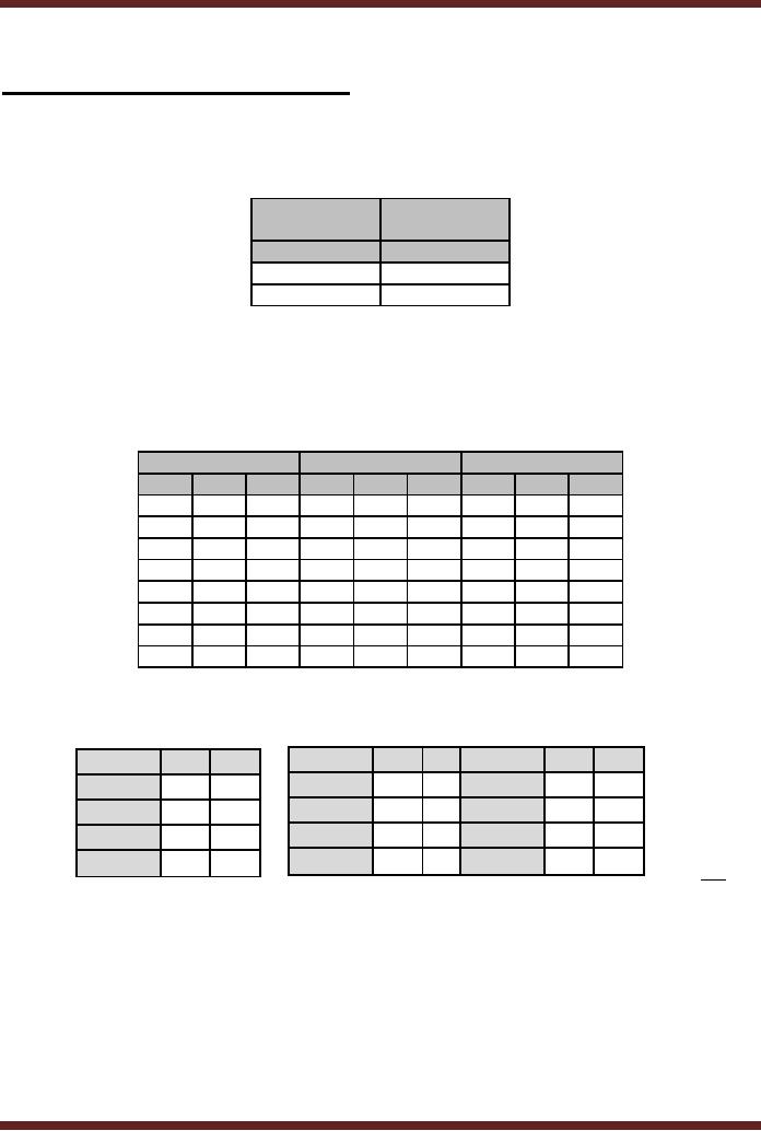
Flip-Flop Transition Table
To implement the counter using D flip-flops instead of J-K flip-flops, the D transition
table is used. The D flip-flop only has a single input and the output of the D flip-flop follows the
input. The D flip-flop transition table is shown. Table 32.1
Flip-flop
Output
Inputs
Transitions
D
Q t+1
1
1
0
0
Table 32.1
D flip-flop Transition table
Karnaugh Maps
The D input table is shown in table 32.2. The Karnaugh maps for the input expressions
are also derived from the input table.
Present State
Next State
D flip-flop inputs
Q 2
Q 1
Q 0
Q 2
Q 1
Q 0
D 2
D 1
D 0
0
0
0
0
0
1
0
0
1
0
0
1
0
1
0
0
1
0
0
1
0
0
1
1
0
1
1
0
1
1
1
0
0
1
0
0
1
0
0
1
0
1
1
0
1
1
0
1
1
1
0
1
1
0
1
1
0
1
1
1
1
1
1
1
1
1
0
0
0
0
0
0
Table 32.2
D flip-flop input table
Q 2 Q 1 /Q 0
0
1 Q 2 Q 1 /Q 0
0
1
Q 2 Q 1 /Q 0
0
1
00
0
1
00
1
0
00
0
0
01
1
0
01
1
0
01
0
1
11
1
0
11
1
0
11
1
0
10
0
1
10
1
0
10
1
1
D 2 = Q 2 ⊕ Q 1 Q 0
D 1 = Q 0 ⊕ Q 1
D 0 = Q 0
Table 32.3
Karnaugh Map for D 2 , D 1 and D 0 inputs
Logic expressions for Flip-flop Inputs
Simplified expressions for D 2 , D 1 and D 0 are obtained from the Karnaugh maps. The
expressions are shown along with the Karnaugh maps.
327
CS302 - Digital Logic & Design
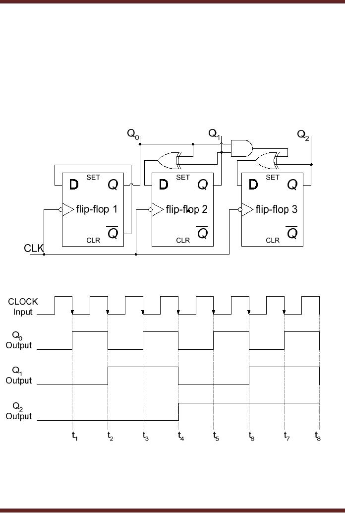
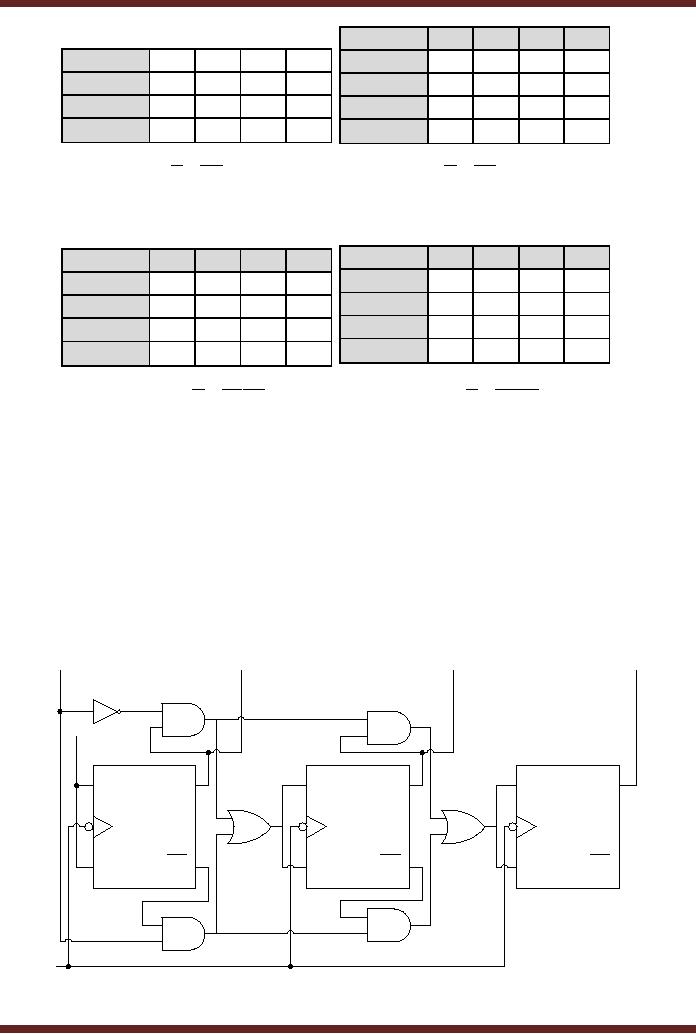
Sequential Circuit Implementation
The first D flip-flop is connected to toggle at each clock transition. The second flip-flop
sets its output depending on the D input. The input to the second flip-flop is determined by the
expression D 1 = Q 0 ⊕ Q 1 , thus at intervals t1 , t 4 , t 5 and t 8 the input D 1 is at logic 1 therefore on
the clock transition the output Q 1 is also set to logic 0. At intervals t 2 , t 3 , t 6 and t 7 the output Q 1
is set to logic 1 as the input D 1 is at logic 1. The input to the second flip-flop is determined by
the expression D 2 = Q 2 ⊕ Q 1 Q 0 , thus at intervals t1 , t 2 , t 3 and t 8 the output Q 2 is set to 0 as D 2
input is at logic 0. At intervals t 4 , t 5 , t 6 and t 7 the output Q 2 is set to logic 1 as D 2 input is at logic
1. Figure 32.1
Figure 32.1a D flip-flop based implementation of 3-bit Synchronous Counter
Figure 32.1b Timing diagram of the D flip-flop based 3-bit Synchronous Counter
Implementing a 3-bit Up/Down Counter
328
CS302 - Digital Logic & Design
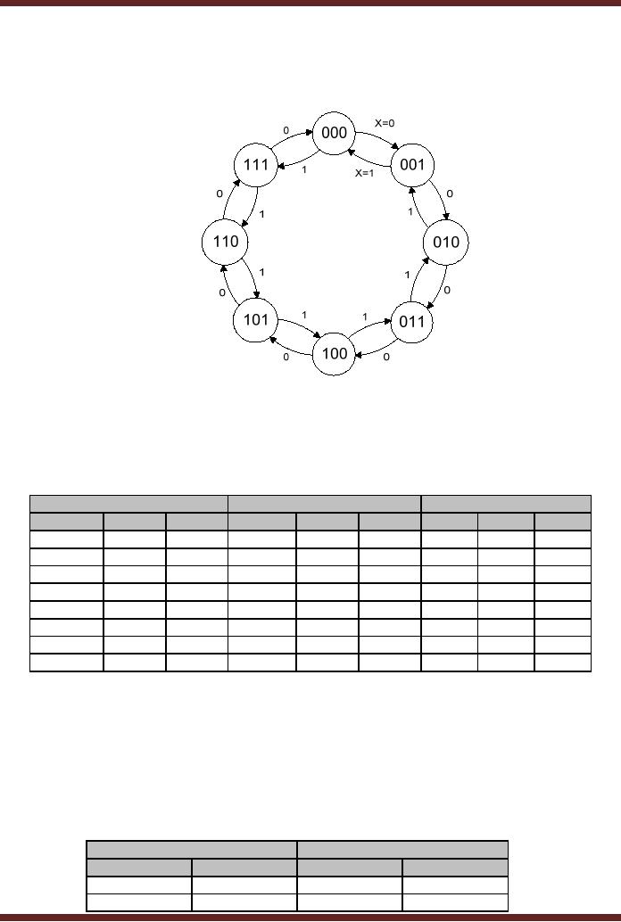
7. State Diagram
The state diagram of a 3-bit Up/Down Synchronous Counter is shown in the figure.
32.2. X=0 and X =1 indicates that the counter counts up when input X = 0 and it counts down
when X =1. X is used as input variable to configure the counter as up or down counter.
Figure 32.2
State diagram of a 3-bit Up-Counter
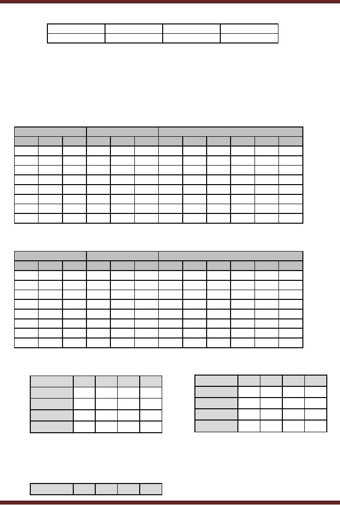
8. Next-State Table
The next state is the state to which the sequential circuit switches when a clock
transition occurs. Table 32.4. The next state outputs for X=0 and X=1 are shown separately.
Present State
Next State X=0
Next State X=1
Q 2
Q 1
Q 0
Q 2
Q 1
Q 0
Q 2
Q 1
Q 0
0
0
0
0
0
1
1
1
1
0
0
1
0
1
0
0
0
0
0
1
0
0
1
1
0
0
1
0
1
1
1
0
0
0
1
0
1
0
0
1
0
1
0
1
1
1
0
1
1
1
0
1
0
0
1
1
0
1
1
1
1
0
1
1
1
1
0
0
0
1
1
0
Table 32.4
Next-State Table for a 3-bit Up-Counter
9. Flip-flop Transition Table
The flip-flop transition table is based on the J-K flip-flop. Table 32.5
Flip-flop Inputs
Output Transitions
J
K
Q t
Q t+1
0
x
0
0
1
x
0
1
329
CS302 - Digital Logic & Design
x
1
1
0
x
0
1
1
Table 32.5
J-K flip-flop Transition table
10. Karnaugh Maps
The J-K flip-flop inputs when state variables change when X=0 and X=1 are shown in
the table 32.6. The J-K inputs can be directly mapped to 4-Variable Karnaugh maps. Table
32.7
Present State
Next State X=0
J-K flip-flop inputs
Q 2
Q 1
Q 0
Q 2
Q 1
Q 0
J 2
K 2
J 1
K 1
J 0
K 0
0
0
0
0
0
1
0
x
0
x
1
x
0
0
1
0
1
0
0
x
1
x
x
1
0
1
0
0
1
1
0
x
x
0
1
x
0
1
1
1
0
0
1
x
x
1
x
1
1
0
0
1
0
1
x
0
0
x
1
x
1
0
1
1
1
0
x
0
1
x
x
1
1
1
0
1
1
1
x
0
x
0
1
x
1
1
1
0
0
0
x
1
x
1
x
1
Table 32.6aJ-K flip-flop input table for X=0
Present State
Next State X=1
J-K flip-flop inputs
Q 2
Q 1
Q 0
Q 2
Q 1
Q 0
J 2
K 2
J 1
K 1
J 0
K 0
0
0
0
1
1
1
1
x
1
x
1
x
0
0
1
0
0
0
0
x
0
x
x
1
0
1
0
0
0
1
0
x
x
1
1
x
0
1
1
0
1
0
0
x
x
0
x
1
1
0
0
0
1
1
x
1
1
x
1
x
1
0
1
1
0
0
x
0
0
x
x
1
1
1
0
1
0
1
x
0
x
1
1
x
1
1
1
1
1
0
x
0
x
0
x
1
Table 32.6bJ-K flip-flop input table for X=1
Q 2 Q 1 /Q 0 X
00
01
11
10
Q 2 Q 1 /Q 0 X
00
01
11
10
00
x
x
x
x
00
0
1
0
0
01
x
x
x
x
01
0
0
0
1
11
0
0
0
1
11
x
x
x
x
10
0
1
0
0
10
x
x
x
x
J 0 = 1
K 0 = 1
Table 32.7a
Karnaugh Map for J 2 and K 2 inputs
Q 2 Q 1 /Q 0 X
00
01
11
10
330
CS302 - Digital Logic & Design
Q 2 Q 1 /Q 0 X
00
01
11
10
00
0
1
0
1
00
x
x
x
x
01
x
x
x
x
01
0
1
0
1
11
x
x
x
x
11
0
1
0
1
10
0
1
0
1
10
x
x
x
x
J 1 = Q 0 X + Q 0 X
K 1 = Q 0 X + Q 0 X
Table 32.7b
Karnaugh Map for J 1 and K 1 inputs
Q 2 Q 1 /Q 0 X
00
01
11
10
Q 2 Q 1 /Q 0 X
00
01
11
10
00
x
x
1
1
00
1
1
x
x
01
x
x
1
1
01
1
1
x
x
11
x
x
1
1
11
1
1
x
x
10
x
x
1
1
10
1
1
x
x
J 2 = Q 1 Q 0 X + Q 1 Q 0 X
K 2 = Q 1 Q 0 X + Q 1 Q 0 X
Table 32.7c
Karnaugh Map for J 0 and K 0 inputs
11. Logic expressions for Flip-flop Inputs
Simplified expressions for J 2 -K 2 , J 1 -K 1 and J 0 -K 0 are directly obtained from the
Karnaugh maps. The expressions are shown along with the Karnuagh maps.
12. Sequential Circuit Implementation
The Boolean expressions obtained in the previous step are implemented using logic
gates. The sequential circuit implemented is shown in figure 32.3
X=0 (up)
Q 0
Q 1
Q 2
X=1 (down)
1
SET
SET
SET
J
Q
J
Q
J
Q
flip-flop 2
flip-flop 1
flip-flop 3
K
Q
K
Q
K
Q
CLR
CLR
CLR
CLK
Figure 32.3
Implementation of the Sequential Circuit
331
CS302 - Digital Logic & Design
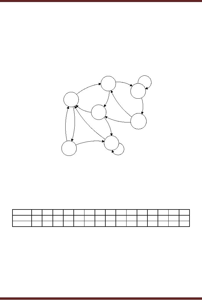
State Reduction
A state diagram show the sequence of current and next states through which the state
machine sequences. Figure 32.4. The transition from a current state to the next state is
determined by current state and the inputs. The outputs of the state machine may also change
during the transition from the current state to the next state. The outputs may depend only on
the current state (Moore Machine) or a combination of current state and the inputs (Mealy
Machine). It is possible that two or more states are equivalent. Two states are considered
equivalent if for the same set of inputs the states change to the same next state or equivalent
next states and give identical outputs. If equivalent states exist then one of the equivalent state
is removed. Reduction in the number of state results in fewer flip-flops and a simpler circuit.
1/0
0/1
a
0/0
b
e
0/0
0/0
1/1
1/0
f
1/1
c
1/0
0/1
1/1
0/0
d
0/0
g
1/0
Figure 32.4
State diagram
Reduction in the number of states is possible if one is interested only in the input and
output relationship, that is, input and outputs remain unchanged. When external outputs are
taken directly from flip-flops, the output must be independent of the number of states before
state reduction algorithms are applied. Consider the sequence a, b, c, f, d, d, e, g, e, g, d, e, a,
f, d, e, a starting from the initial state a. The inputs and the corresponding outputs are shown
in the table. Table 32.8
state
a
b
c
f
d
d
e
g
d
e
a
f
d
e
a
Input
1
1
1
0
1
0
1
0
0
0
0
0
0
0
Output
0
1
1
0
0
1
1
0
1
0
0
0
1
0
Table 32.8
The input and output sequence
In the next state table the state `f' is equivalent to state `g' as for each set of inputs
states `f' and `g' change to states `d' and `e' respectively. Table 32.9a. Similarly, the outputs
also remain identical. Therefore state `g' can be eliminated and in the state table all instances
of state `g' are replaced by state `f'.
332
CS302 - Digital Logic & Design
Present
Next State
Output
State
X=0
X=1
X=0
X=1
a
f
b
0
0
b
b
c
1
1
c
a
f
0
1
d
e
d
1
0
e
a
g
0
1
f
d
e
0
0
g
d
e
0
0
Table 32.9a
Next-State table
Present
Next State
Output
State
X=0
X=1
X=0
X=1
a
f
b
0
0
b
b
c
1
1
c
a
f
0
1
d
e
d
1
0
e
a
f
0
1
f
d
e
0
0
Table 32.9b
Next State table, with state `g' eliminated and instances of state `g' replaced by
state `f'
In the next state table state `c' is equivalent to state `e' as for each input, the current
state changes to the same next states. Table 32.9b. The outputs are also identical when
changing from the present state to the next state. The state table is simplified by eliminating
state e and replacing all instances of state `e' with state `c'. table 32.9c. The State diagram
represented by the simplified state table is shown. Figure 31.7.
Present
Next State
Output
State
X=0
X=1
X=0
X=1
a
f
b
0
0
b
b
c
1
1
c
a
f
0
1
d
c
d
1
0
f
d
c
0
0
Table 32.9c
Next State table, with state `e' eliminated and instances of state `e' replaced by
state `c'
333
CS302 - Digital Logic & Design
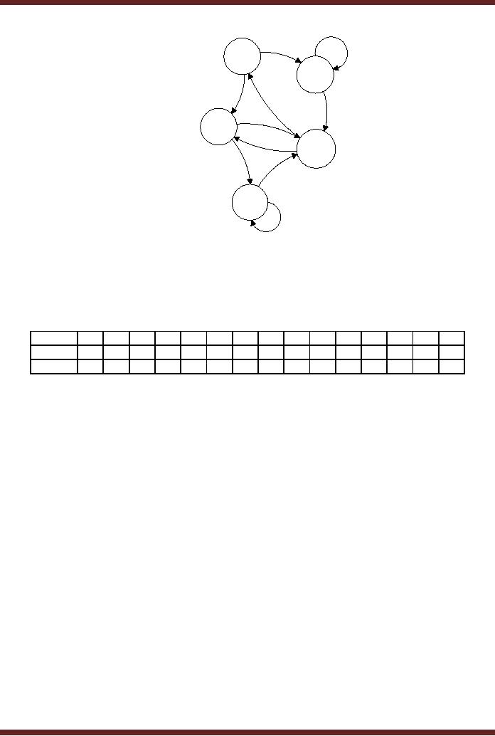
1/0
0/1
a
b
0/0
0/0
1/1
1/0
f
1/1
c
0/0
0/1
d
1/0
Figure 32.5
Simplified State diagram
Reconsider the initial sequence a, b, c, f, d, d, e, g, e, g, d, e, a, f, d, e, a starting from
the initial state a. The inputs and outputs for the state sequence derived from the simplified
State diagram are shown in table 32.10.
state
a
b
c
f
d
d
c
f
d
c
a
f
d
c
a
Input
1
1
1
0
1
0
1
0
0
0
0
0
0
0
Output
0
1
1
0
0
1
1
0
1
0
0
0
1
0
Table 32.10
The input and output sequence obtained from the simplified state diagram
Elimination of equivalent states results in the reduction in the number of flip-flops. In
the example described, the elimination of two states reduces the total number of unique states
from seven to five, however the number of flip-flops remain the same which is three. If the
number of states had been reduced to four then only two flip-flops would be required.
334
- AN OVERVIEW & NUMBER SYSTEMS
- Binary to Decimal to Binary conversion, Binary Arithmetic, 1�s & 2�s complement
- Range of Numbers and Overflow, Floating-Point, Hexadecimal Numbers
- Octal Numbers, Octal to Binary Decimal to Octal Conversion
- LOGIC GATES: AND Gate, OR Gate, NOT Gate, NAND Gate
- AND OR NAND XOR XNOR Gate Implementation and Applications
- DC Supply Voltage, TTL Logic Levels, Noise Margin, Power Dissipation
- Boolean Addition, Multiplication, Commutative Law, Associative Law, Distributive Law, Demorgan�s Theorems
- Simplification of Boolean Expression, Standard POS form, Minterms and Maxterms
- KARNAUGH MAP, Mapping a non-standard SOP Expression
- Converting between POS and SOP using the K-map
- COMPARATOR: Quine-McCluskey Simplification Method
- ODD-PRIME NUMBER DETECTOR, Combinational Circuit Implementation
- IMPLEMENTATION OF AN ODD-PARITY GENERATOR CIRCUIT
- BCD ADDER: 2-digit BCD Adder, A 4-bit Adder Subtracter Unit
- 16-BIT ALU, MSI 4-bit Comparator, Decoders
- BCD to 7-Segment Decoder, Decimal-to-BCD Encoder
- 2-INPUT 4-BIT MULTIPLEXER, 8, 16-Input Multiplexer, Logic Function Generator
- Applications of Demultiplexer, PROM, PLA, PAL, GAL
- OLMC Combinational Mode, Tri-State Buffers, The GAL16V8, Introduction to ABEL
- OLMC for GAL16V8, Tri-state Buffer and OLMC output pin
- Implementation of Quad MUX, Latches and Flip-Flops
- APPLICATION OF S-R LATCH, Edge-Triggered D Flip-Flop, J-K Flip-flop
- Data Storage using D-flip-flop, Synchronizing Asynchronous inputs using D flip-flop
- Dual Positive-Edge triggered D flip-flop, J-K flip-flop, Master-Slave Flip-Flops
- THE 555 TIMER: Race Conditions, Asynchronous, Ripple Counters
- Down Counter with truncated sequence, 4-bit Synchronous Decade Counter
- Mod-n Synchronous Counter, Cascading Counters, Up-Down Counter
- Integrated Circuit Up Down Decade Counter Design and Applications
- DIGITAL CLOCK: Clocked Synchronous State Machines
- NEXT-STATE TABLE: Flip-flop Transition Table, Karnaugh Maps
- D FLIP-FLOP BASED IMPLEMENTATION
- Moore Machine State Diagram, Mealy Machine State Diagram, Karnaugh Maps
- SHIFT REGISTERS: Serial In/Shift Left,Right/Serial Out Operation
- APPLICATIONS OF SHIFT REGISTERS: Serial-to-Parallel Converter
- Elevator Control System: Elevator State Diagram, State Table, Input and Output Signals, Input Latches
- Traffic Signal Control System: Switching of Traffic Lights, Inputs and Outputs, State Machine
- Traffic Signal Control System: EQUATION DEFINITION
- Memory Organization, Capacity, Density, Signals and Basic Operations, Read, Write, Address, data Signals
- Memory Read, Write Cycle, Synchronous Burst SRAM, Dynamic RAM
- Burst, Distributed Refresh, Types of DRAMs, ROM Read-Only Memory, Mask ROM
- First In-First Out (FIFO) Memory
- LAST IN-FIRST OUT (LIFO) MEMORY
- THE LOGIC BLOCK: Analogue to Digital Conversion, Logic Element, Look-Up Table
- SUCCESSIVE �APPROXIMATION ANALOGUE TO DIGITAL CONVERTER
Design a 3 Bit Synchronous Counter Using D Flip Flop
Source: https://www.zeepedia.com/read.php?d_flip-flop_based_implementation_digital_logic_design&b=9&c=32
0 Response to "Design a 3 Bit Synchronous Counter Using D Flip Flop"
Post a Comment